Reverse Bias V-I Characteristics of PN Junction. What Is a PN Junction When a p-type semiconductor is suitably joined to an n-type semiconductor the contact surface is called pn junction.

P N Junction Wikipedia
Concept behind height of Potential BarrierEnergy Band diagram of Diode under Open circuit conditionEnergy Band diagram of Diode under Forward BiasEnergy Band.
What is meant by pn junction. A PN Junction Diode is one of the simplest semiconductor devices around and which has the characteristic of passing current in only one direction only. Away from the junction the band bending can be computed based on the usual. Obviously the built-in voltage in the PN junction has real-world effects.
A pn junction has two sides a hole-rich p side and an electron-rich n side. A voltage results from the electric field formed at the junction. The result of this process is that the PN junction has rectifying currentvoltage IV or IV characteristics.
A p-n junction diode is two-terminal or two-electrode semiconductor device which allows the electric current in only one direction while blocks the electric current in opposite or reverse direction. What is pn junction diode in physics. Formation of a PN-Junction.
Most semiconductor devices contain one or more pn junctions. Once the applied voltage is increased to a value where the reverse voltage across the diode reaches the breakdown value of the diode which is VBR the reverse current. Semiconductor interfaces can be organized into three types of heterojunctions.
The PN voltage is really in there but we cant get at it with normal meters since its being canceled by the metal-semiconductor contacts. A p-n junction diode is a basic semiconductor device that controls the flow of electric current in a circuit. All PN junctions are automatically biased by this built-in voltage.
Formation of pn Junction In actual practice a pn junction will. When a p-type semiconductor is suitably joined to n-type semiconductor the contact. Answer 1 of 9.
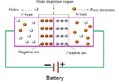
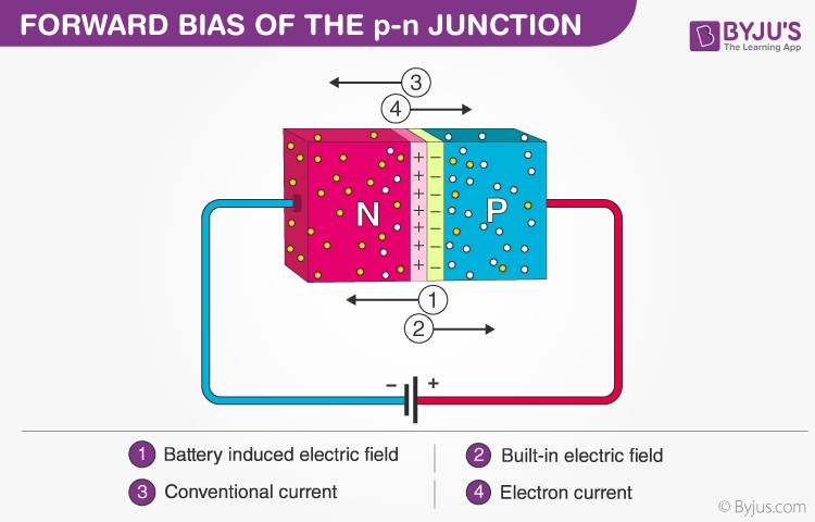
In a reverse-biased PN junction the N-type side has positive and the P-type side has negative. Our diodes turn on at around 06Vdc. A PN junction is said to be forward-biased when the p-type region of a junction is connected to the positive terminal of a voltage source and the n-type region is connected to the voltage sources negative terminal.
The Zener and Avalanche breakdown both occur in diode under reverse bias. A PN junction diode is a non-linear component and it consists of two junctions namely P-junction N-junction where the majority and minority charge carriers are present like electrons and holes. P-n junctions are formed by joining n-type and p-type semiconductor materials as shown below.
In this case the minority negative carriers are pulled towards the positive side and the minority positive carriers are pulled towards the negative side the depletion zone widen. The Avalanche Breakdown and Zener Breakdown are two different mechanisms by which a PN junction breaks. Potential barrier is the potential difference or junction voltage developed across the junction due to migration of majority charge carriers across it when p-n junction.
When the positive voltage is applied to the p- type side it shrinks and overcome the de. What Is Meant By Junction Diode August 24 2019 Get link. On the p side holes are the majority carriers and electrons are minority carriers.
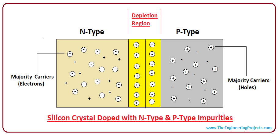
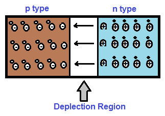
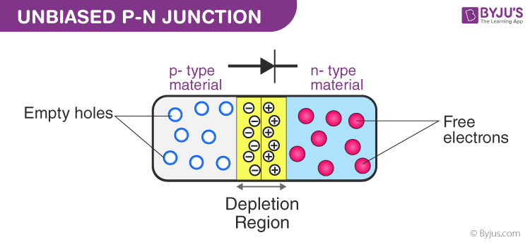
A diode is a PN junction with p-type of one side n- type on the other. Most semiconductor devices contains one or more pn junctions. Depletion layer is the region created around the p-n junction which is devoid of free charge carriers and has immobile ionsIt is created due to diffusion of majority carriers across the junction when p-n junction is formed.
The p-n junction which is formed when the p-type and n-type semiconductors are joined is called as p-n. This diode includes two terminals namely anode and cathode where a p-type semiconductor is an anode. A PN junction diode is a two-terminal or two-electrode semiconductor device A diode is called as P-N junction diode if it is formed by P-type on one side and N-type on the supplementary one or reverse direction.
Both types of carriers exist but in vastly different quantities so that the product of their concentration pn is a constant d. Straddling gap type I staggered gap type II or broken gap type III as seen in the figure. By applying a negative voltage reverse bias results in the free charges being pulled away from the junction resulting in the depletion layer width being increased.
The avalanche breakdown occurs because of the ionisation of electrons and hole pairs whereas the Zener diode occurs because of heavy doping. Surface is called pn junction. Pn Junction Diode And Its Forward Bias Reverse Bias.
It is also known as a semiconductor diode or PN junction diode. PN Junction Distance Then the presence of impurity ions on both sides of the junction cause an electric field to be established across this region with the N-side at a positive voltage relative to the P-side. The behaviour of a semiconductor junction depends crucially on the alignment of the energy bands at the interface.
The pn junction is of great importance as it is the main control element for the semiconductor devices. Forward Biased PN Junction. It has a positive p side and a.
Of great importance because it is in effect the control element for semiconductor. In this forward-biased condition due to the attraction of the positive terminal of the source electrons that participated in. The pn junction is.
Resulting in an electron field at the junction and forming the depletion region. When a reverse bias is applied across a PN junction there is an extremely small reverse current IR through the PN junction due to minority carriers.

Pn Junction Theory For Semiconductor Diodes

Pn Junction Diode And Diode Characteristics
Introduction To Pn Junction The Engineering Projects
Pn Junction Definition Formation Application Vi Characteristics And Faqs
Vi Characteristics Of Pn Junction Diode In 3 Biasing Modes

Pn Junction Diode And Diode Characteristics
Pn Junction Diode And Its Working Principle Electrical Concepts

P N Junction Semiconductor Diode Diode
Pn Junction Definition Formation Application Vi Characteristics And Faqs

P N Junction Wikipedia

P N Junction Diode Definition Properties Video Lesson Transcript Study Com

Basic Semiconductor Electronics Pn Junction Diode Dr Pankaj

Pn Junction Diode

Forward And Reverse Bias Of A Pn Junction Explained Electrical4u

Pn Junction What Is It And How To Make One Electrical4u

Pn Junction Diode Characteristics Lab Expriment

P N Junction Wikipedia

Pn Junction Theory For Semiconductor Diodes

Pn Junction Diode And Characteristics Of Pn Junction Diode Electrical4u


Post a Comment
Post a Comment